Table of Content:
| Semiconductors | Depletion Region Definition | Forward Bias and Reverse Bias |
What is the meaning of depletion? The word depletion in English refers to the decrease in the quantity of something. Similarly, in semiconductors, the depletion region is the layer where the flow of charges decreases. This region acts as the barrier that opposes the flow of electrons from the n-side to the p-side of the semiconductor diode.
Download Complete Chapter Notes of Semiconductors and electronic devices
Download Now
Semiconductors
Semiconductors are materials that have electrical properties somewhere in the middle of a conductor and an insulator. Two common examples of semiconductors are silicon (Si) and germanium (Ge). The conductivity of the semiconductor is improved by a process called doping. Doping is the method of adding impurities to the semiconductor material. Depending on the type of impurities added, the semiconductor will become p-type or n-type. The semiconductors in which the impurities are not added are called pure or intrinsic semiconductors and the semiconductors with impurities are called extrinsic semiconductors
The p-type semiconductor is formed by adding trivalent impurities like aluminium, boron or indium to the intrinsic semiconductor. The majority charges are the holes in p-type semiconductors. In an n-type semiconductor, the pentavalent impurities like arsenic, antimony or phosphorus are used as impurities. In n-type semiconductors, the electrons are the majority charge carriers.
What is a depletion region? – Depletion Region Definition
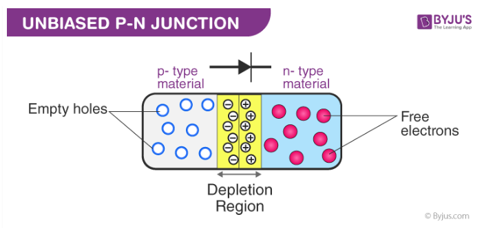
When the p-type and the n-type materials are kept in contact with each other, the junction between them behaves differently from either side of the material alone. The electrons and holes are close to each other at the junction. According to coulomb’s law, there is a force between the negative electrons and the positive holes. When the p-n junction is formed a few electrons from the n-type diffuse through the junction and combines with the holes in the p-side to form negative ions and leaves behind positive ions in the n-side. This results in the formation of the depletion layer, which acts as the barrier and does not allow any further flow of electrons from the n region to the p region.

Forward Bias and Reverse Bias
In the forward bias, the p side of the diode is connected to the positive side of the battery and the n side is connected to the negative side of the battery. The direction of the applied voltage is opposite to the junction barrier potential. Therefore, the size of the depletion region decreases. Therefore, the voltage applied in the forward direction assists the electrons in the n region to overcome the barrier and flow to the p region.
When the p-side is connected to the negative terminal and n-side is connected to the positive terminal of the battery, it is called reverse biased. When a reverse bias is applied, free electrons are pulled away from the junction, which results in the increase of the width and resistance of the depletion region.

Thank you so much. Important information about NEET. Thank you so much.