A conduction band is a delocalised band of energy levels in a crystalline solid that is partially filled with electrons. These electrons are highly mobile and are responsible for electrical conductivity. However, before we learn about the conduction band, we will understand the band theory.
Table of Contents
- Band Theory
- What Is the Conduction Band?
- Conduction Bands in Semiconductors and Metallic Conduits
- Differences between Valence Band and Conduction Band
- Forbidden Band
- Understanding Related Terms
- Conduction Band Questions
- Frequently Asked Questions – FAQs
Band Theory
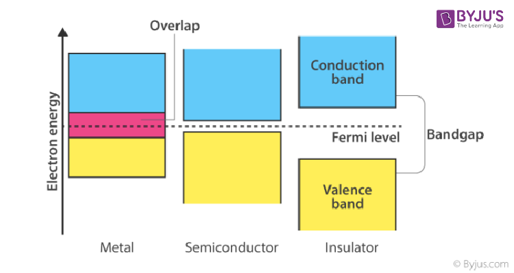
A useful way to visualise the distinction between conductors (metal), insulators and semiconductors is to plot out their energies for electrons within the material. Rather than having distinct energies, as within the case of free atoms, the energy states which are available form bands.
Crucial to the conductivity method is whether or not the electrons are inside the conductivity band. In insulators, the electrons inside the valence band are separated by a large gap from the conduction band; in conductors, like metals, the valence band overlaps the conduction band, and in semiconductors, there is a very little gap between the valence and conduction bands that thermal or totally different excitations can bridge the gap.
With such a small gap, the presence of a less proportion of doping material can increase conduction dramatically. A vital parameter inside the band theory is that of the Fermi level, the highest of the accessible electron energy levels at lower temperatures. The position of the Fermi level in relevance to the conductivity band might be important to place confidence in crucial electrical properties.
What Is the Conduction Band?
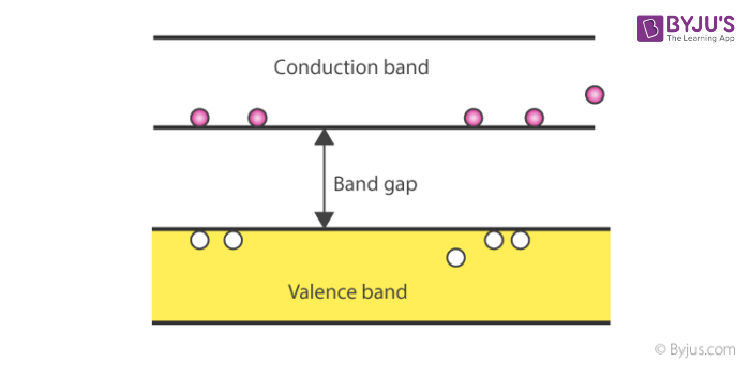
The conduction band is the band of electron orbitals that electrons can bounce up into from the valence band when energised. At the point when the electrons are in these orbitals, they have enough energy to move freely in the material. This movement of electrons makes an electric current flow. The valence band is the furthest electron orbital of a particle of a particular material in which electrons are involved.
Also Read: Basic Logic Gates
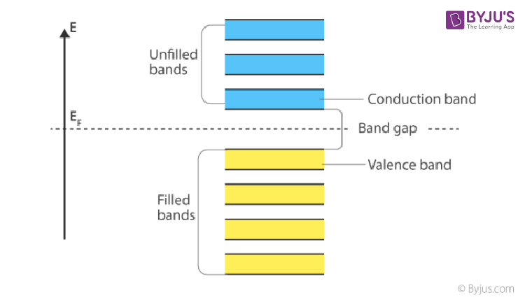
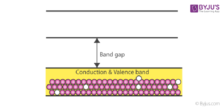
The energy distinction between the highest occupied energy state of the valence band and the least abandoned condition of the conduction band is known as the bandgap, and is demonstrative of the electrical conductivity of a material. An enormous bandgap implies that a great deal of vitality is required to energise valence electrons to the conduction band. Then again, when the valence band and conduction band cover as they do in metals, electrons can promptly bounce between the two groups, which means the material is profoundly conductive.
The electrons in this energy band can expand their energies by going to higher energy levels inside the band when an electric field is applied to quicken them or when the temperature of the crystal is increased. These electrons are called conduction electrons.
Conduction Bands in Semiconductors and Metallic Conductors
In metallic conductors, the conduction band and the valence band overlap.
In semiconductors and inductors at adequately low temperatures, the conduction band has no electrons. Conduction electrons originate from the thermal excitation of electrons from a lower energy band or from impurity atoms in the crystal.
Valence Band and Conduction Band
Here are some of the differences between a valence band and a conduction band.
| Conduction Band | Valence Band |
| Higher energy level band | An energy band is formed by a series of energy levels containing valence electrons |
| Partially filled by the electrons | Always filled with electrons |
| High energy state | Low energy state |
| Above the Fermi level | Below of Fermi level |
| Electrons move into the conduction band when the atom is excited | Electrons will move out of the conduction band when the atom is excited |
| Current flows due to such electrons | The highest energy level, which can be occupied by an electron in the valence band at 0 K |
Forbidden Band
The forbidden band is the energy gap between a conduction band and a valence band. Some of its characteristics include the following:
- No free electron is present.
- No energy.
- The width of the forbidden energy gap depends upon the nature of the substance.
- As temperature increases (↑), the forbidden energy gap decreases (↓) very slightly.
Understanding Related Terms
Conduction Electrons
Electrons are allowed to move inside a solid. The movement of these electrons can offer ascent to the conduction of power by making an electric flow through the solid.
Conductor
A material with low resistivity is utilised for contacts and interconnects in semiconductor preparation. The conduction band and the valence band overlap in a conductor. In this way, in a conductor, the conduction band is equivalent to the valence band, and the charge bearers are fundamentally electrons.
Conductivity (s)
The measure of how freely current can flow through a material is called conductivity. Copper, with its high conductivity of 5.95 x 10⁷ W-1m-1, conveys electric flow more freely than aluminium, with its marginally lower conductivity of 3.77 x 10⁷ W-1m-1. Conductivity is the converse of resistivity r:
s = 1/r.
Also Read: Working of Transistors
Mobility
It describes the ease with which charge carriers drift in the material
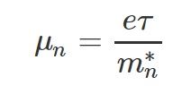
Where e is the charge of the electron, τ is the relaxation time, and m*n is the mass of the electron.
Conduction Band Questions
1. Electrons from the valence band rise to the conduction band when the temperature is greater than 0 k. Is it True or False?
a) True
b) False
Answer: a
Explanation: As the temperature rises above 0 k, the electrons gain energy and rise to the conduction band from the valence band.
2. The thermal equilibrium concentration of the electrons in the conduction band and the holes in the valence band depend upon ______.
a) Effective density of states
b) Fermi energy level
c) Both A and B
d) Neither A nor B
Answer: c
Explanation: The electrons and holes depend upon the effective density of the states and the Fermi energy level.
3. What is the SI unit of conductivity?
a) Ωm
b) (Ωm)-1
c) Ω
d) m
Answer: b
Explanation: The formula of the conductivity is the σ = 1/ρ.
So, the unit of resistivity is Ωm.
Now, the unit of conductivity becomes the inverse of resistivity.
4. In an insulator, the forbidden energy gap between the valence band and conduction band is of the order of:
A) 1MeV
B) 0.1MeV
C) 1eV
D) 5eV
Answer: D
Explanation: In insulators, the forbidden energy gap is the largest, and it is of the order of 5 eV.
5. The forbidden energy bandgap in conductors, semiconductors, and insulators are EG1, EG2, and EG3, respectively. The relation among them is:
A) EG1=EG2=EG3
B) EG1<EG2<EG3
C) EG1>EG2>EG3
D) EG1<EG2>EG3
Answer: B
Explanation: In insulators, the forbidden energy gap is very large; in the case of semiconductors, it is moderate, and in conductors, the energy gap is zero.
6. The forbidden gap in the energy bands of germanium at room temperature is about:
A) 1.1eV
B) 0.1eV
C) 0.67eV
D) 6.7eV
Answer: C
Explanation: (Germanium) = 0.67eV
Semiconductors Video Lesson – Important Topics

Semiconductors Important JEE Main Questions


Comments