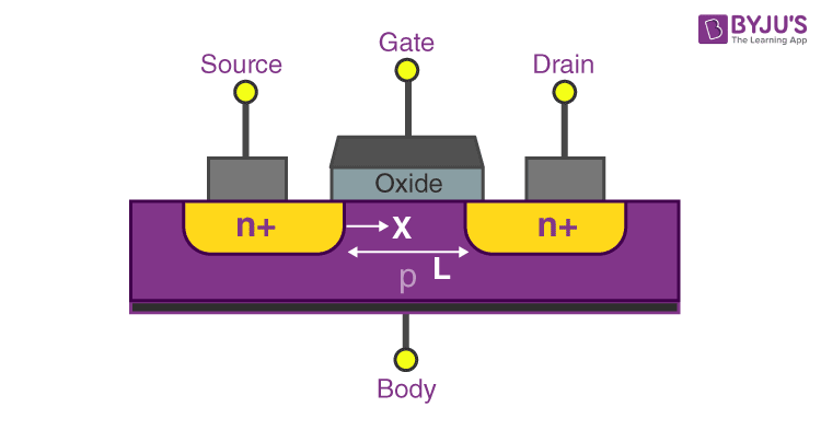
Field-effect transistors (FETs) are crucial electronic components in modern electronics. FETs offer several advantages, such as low power consumption, high input impedance, and simple biasing requirements. In this article, we will delve into the history of FETs, from the early inventions and patents to the modern developments and applications. We will also explore the types of FETs, their working principles, and their key specifications.
| Table of Contents |
FET Basics
Field-Effect Transistor (FET) is a semiconductor device that consists of a channel made of a semiconductor material, with two electrodes connected at either end, namely the drain and the source. The flow of current between the source and the drain terminals is controlled by a third electrode, known as the gate, which is placed in close proximity to the channel. By applying a voltage at the gate terminal, the number of charge carriers in the channel can be modulated, leading to a corresponding change in the current flow between the source and the drain terminals. The FET is classified into two types based on its mode of operation, namely the enhancement mode and depletion mode FETs, depending on whether the voltage applied at the gate terminal increases or decreases the current flow through the channel.
FET Working
When a voltage is applied to the gate electrode, an electric field is created across the insulating layer, which in turn creates a depletion region in the channel. The depletion region reduces the number of free charge carriers in the channel, and thus the conductivity of the channel is reduced. This effect is known as the field-effect, and it is the basis of the FET operation. In the case of an n-type FET, a negative voltage applied to the gate electrode creates a depletion region in the channel, which reduces the flow of electrons from the source to the drain. In contrast, a positive voltage applied to the gate electrode of a p-type FET creates a depletion region that reduces the flow of holes from the source to the drain. Thus, by varying the voltage applied to the gate electrode, the conductivity of the channel can be controlled, and the flow of current through the FET can be modulated.
To explain the working principle of FET, the analogy of a water pipe and vessel can be used. In this analogy, the source of water can be considered as the source terminal of FET, while the vessel that collects water can be analogous to the drain terminal of FET. The gate terminal can be compared to the controlling tap that regulates the flow of water. Similar to how the tap modulates the flow of water, the voltage applied at the gate terminal controls the flow of current from the source to the drain terminal of FET. Thus, the FET operates by controlling the flow of current through the channel by modulating the number of charge carriers in the channel using the voltage applied at the gate terminal.
History of FET Transistor
Julius Edgar Lilienfeld was the first to file a patent for a field-effect transistor in 1926, however, his device faced significant technical challenges that hindered its practical application. The design of Lilienfeld’s device relied on a thin metal film as a gate, which was deposited onto a semiconductor substrate. Unfortunately, the quality of the metal-to-semiconductor contact was poor, resulting in high resistance and low device efficiency. Additionally, the insulating layer used in Lilienfeld’s device was unstable, making it unsuitable for high-voltage applications. Therefore, there was a need to improve the device design to overcome these limitations and make it practical for real-world applications. In 1934, Oskar Heil also filed a patent for a similar device. Oskar Heil’s device was not rejected per se, but it was not as successful as Lilienfeld’s device in practical implementation. Lilienfeld’s device used a thin layer of metal oxide to form the gate of the transistor, while Heil’s device used a metal-semiconductor junction. The metal-semiconductor junction was more difficult to produce and control than the metal oxide layer, which limited the practicality of Heil’s device.
Additionally, Heil’s device was not widely known or recognized at the time, and it was only after the development of the junction transistor by Shockley and his team at Bell Labs that the potential of field-effect transistors was fully realized. Nonetheless, Heil’s contributions to developing FETs were significant, and his work paved the way for later technological advancements. However, the first working field-effect transistor, called the junction gate field-effect transistor, was developed by William Shockley and his team at Bell Labs in 1947. Shockley and his colleagues John Bardeen and Walter Brattain were awarded the Nobel Prize in Physics in 1956 for inventing the junction transistor, which included the junction gate field-effect transistor as a key component. Since then, field-effect transistor technology has undergone significant developments, making it one of the most important electronic components of the 20th and 21st centuries.
Essential Information concerning FETs

Field-effect transistors (FETs) can be classified into two types: majority carrier devices, where the current is carried primarily by the majority carriers, and minority carrier devices, where the current flow is primarily due to the minority carriers. In FETs, electrons flow from the source to the drain through active channels in the device, and ohmic contacts connect both the terminal conductors to the semiconductor material. The source terminal and the gate have a potential between them, and the conductivity of the channel is a function of this potential.
FETs have three terminals:
- The first terminal is the source (S), through which current enters the device, denoted by IS.
- The second terminal is the drain (D), through which current leaves the device, denoted by ID. The voltage between drain and source is VDS.
- The third terminal is the gate (G), which modulates the channel conductivity. By applying a voltage at the gate, ID can be controlled.
The names of the terminals are based on their functions, which are similar to real-life gates that control when they open and close. The gate can permit the passage of electrons or block it.
Types of FETs
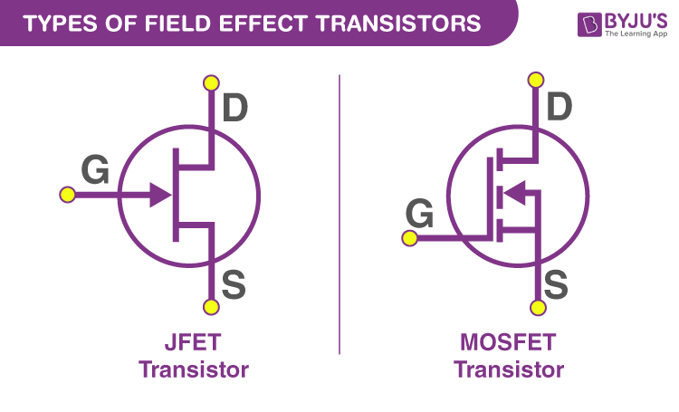
There are two types of Field Effect Transistors:
- Junction Field Effect Transistor (JFET)
- Metal oxide semiconductor Field Effect Transistor (MOSFET)

Junction Field Effect Transistor (JFET)
JFET is one of the most basic forms of field-effect transistors. They are three-terminal semiconductor electrical devices that can act as electronically controlled resistors or switches. Unlike a BJT (bipolar junction transistor), a JFET is voltage-controlled and does not require a biasing electrical current. The full-form JFET is Junction-gate Field Effect Transistor. The JFET controls the current flow between the source and the drain terminals by varying the voltage applied to the gate terminal. When a voltage is applied to the gate terminal, it creates an electric field that controls the width of the depletion region in the channel between the source and the drain terminals.
- When the gate-to-source voltage is zero, the depletion region is narrow, and the channel offers low resistance to the current flow between the source and the drain terminals. This is called the “pinch-off” condition, and the JFET is said to be in saturation.
- When the gate-to-source voltage is decreased in a JFET (junction field-effect transistor), the depletion region around the channel between the source and drain increases in width. This reduces the effective channel width, which in turn, decreases the conductivity of the channel. As a result, the drain current decreases, and the JFET becomes more resistive.
- When the gate-to-source voltage increases in a JFET (junction field-effect transistor), the depletion region around the channel between the source and drain decreases in width. This increases the effective channel width, which in turn, increases the conductivity of the channel. As a result, the drain current also increases, and the JFET becomes less resistive.
Read More: JFET
Metal-Oxide Semiconductor Field-Effect Transistor (MOSFET)
The MOSFET is another type of field-effect transistor (FET) that can switch electronic signals or amplify them. It is made of an insulated gate that controls the device’s conductivity per the voltage applied. This nature makes it useful for switching electronic signals or amplifying by adjusting its conductivity with changing voltage levels.
The crucial advantage of MOSFET is that they require almost no input current to regulate the load current relative to bipolar transistors (BJTs or bipolar junction transistors). There are two types of MOSFETs: enhancement mode and depletion mode. In the case of an enhancement mode MOSFET, the exerted voltage at the gate increases the conductivity. In depletion mode transistors, the voltage exerted at the gate decreases the conductivity.
Read More: MOSFET
Applications of FET
The important applications of MOSFETs are:
- FETs (field effects transistors) are used in constructing mixer circuits to restrict low intermodulation distortions.
- FETs are employed in low-frequency amplifiers because of their relatively small coupling capacitors.
- FET is a voltage-controlled electrical device; due to this, it is utilised in operational amplifiers in the form of variable voltage resistors.
- Due to their large input Impedance, FET is typically used as input amplifiers in electrical devices, i.e. oscilloscopes, voltmeters, and other measuring tools.
- FET is also used to construct radio frequency amplifiers for FM appliances.
- FET is used for the mixer operation of TV and FM receivers.
- Because of their small size, FETs are also used in LSI (large-scale integration) and computer memory modules.

Comments