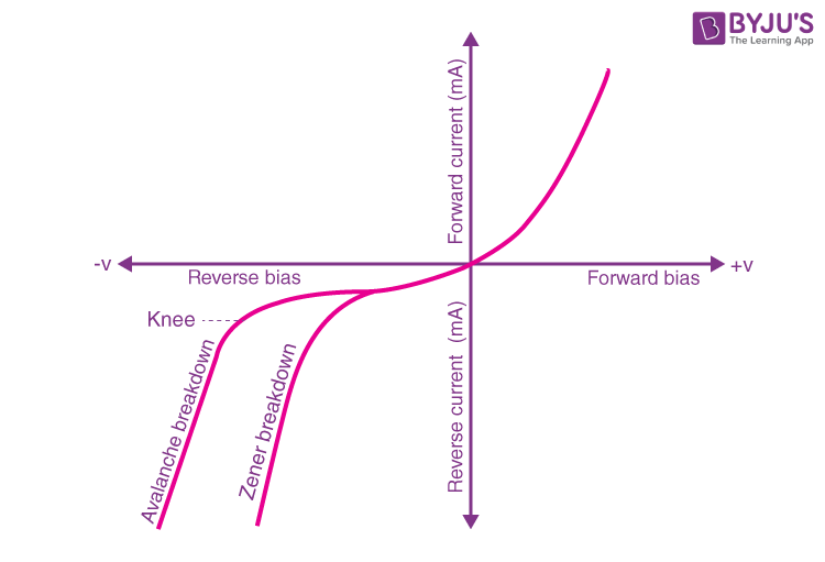
Breakdown diodes can be defined as two-terminal electrical components. Different diodes are available in the market fabricated with semiconductor objects such as Silicon and Germanium. The overall objective of the diode is to allow the current to flow only in one direction and block the current in the reverse direction.
In this session, let us know the difference between Zener breakdown and avalanche breakdown.
| Table of Contents: |
PN Junction Breakdown
An electrical breakdown of any material such as the conductor, semiconductor, and insulator can occur due to two different phenomena known as a) Zener Breakdown b) Avalanche Breakdown.
What Is Zener Breakdown?
When the diode is reverse biased, the kinetic energy of the electrons increases, and they move at a high velocity. The high-velocity electrons collide with other atoms and give rise to free electrons. These free electrons, in turn, give rise to a high value of reverse saturation current. This is known as Zener breakdown.
Read More: Zener Diode
What Is Avalanche Breakdown?
The avalanche breakdown occurs when a high reverse voltage is applied across the diode. As we increase the applied reverse voltage, the electric field across the junction increases. This electric field exerts a force on the electrons at the junction and frees them from covalent bonds. These free electrons start moving with high velocity across the junction and collide with the other atoms, thus creating more free electrons. This results in a rapid increase in net current. Both these breakdowns occur in Zener diodes.

Zener Breakdown vs Avalanche Breakdown
The main difference between Zener breakdown and avalanche breakdown is their mechanism of occurrence. Zener breakdown occurs because of the high electric field. The avalanche breakdown occurs because of the collision of free electrons with atoms. Both these breakdowns can occur simultaneously. Let us look at the other differences between them in the below table.
| The process in which the electrons move across the barrier from the valence band of p-type material to the conduction band of n-type material is known as Zener breakdown. | The process of applying high voltage and increasing the free electrons or electric current in semiconductors and insulating materials is called an avalanche breakdown. |
| This is observed in Zener diodes having a Zener breakdown voltage Vz of 5 to 8 volts. | This is observed in Zener diode having a Zener breakdown voltage Vz greater than 8 volts. |
| The valence electrons are pulled into conduction due to the high electric field in the narrow depletion region. | The valence electrons are pushed to conduction due to the energy imparted by accelerated electrons, which gain their velocity due to their collision with other atoms. |
| The increase in temperature decreases the breakdown voltage. | The increase in temperature increases the breakdown voltage. |
| The VI characteristics of a Zener breakdown has a sharp curve. | The VI characteristic curve of the avalanche breakdown is not as sharp as the Zener breakdown. |
| It occurs in diodes that are highly doped. | It occurs in diodes that are lightly doped. |
The difference between avalanche breakdown and Zener breakdown is important as most of us get confused between the two. To know more about other differences, Visit BYJU’S.
| Similar Difference Between Articles |
Learn more about Semiconductors and Electronic Devices
Frequently Asked Questions – FAQs
Which are the materials used in the fabrication of diodes?
State true or false: in the Zener breakdown, the increase in temperature increases the breakdown voltage.
False. In Zener breakdown, the increase in temperature decreases the breakdown voltage.
In which type of diode avalanche breakdown takes place?
It occurs in diodes that are lightly doped.
Define Zener breakdown?
What happens in avalanche breakdown when the increase in temperature takes place?
Stay tuned to BYJU’S and Fall in Love with Learning!

good and very useful information .thank you.